The CHIPS Act fab boom
The CHIPS and Science Act, signed into law in August 2022, allocated $52.7 billion in federal funding for semiconductor manufacturing and research in the United States. That government commitment unlocked a wave of private capital that now totals well over $300 billion in announced investments. In a single legislative stroke, Washington transformed the US semiconductor landscape from a country that had watched its global fab share fall to roughly 12 percent all the way back to a serious contender for leading-edge production.
The geopolitical motivation is straightforward. Roughly 90 percent of the world's most advanced chips are manufactured in Taiwan, and policymakers in both parties concluded that concentration was a strategic vulnerability. The answer was to triple US fab capacity over roughly a decade, anchoring that expansion in Taiwan Semiconductor Manufacturing Company plants in Phoenix, Intel facilities in Columbus and Chandler, Samsung in Taylor Texas, and Micron in Syracuse New York and Boise Idaho. Each of those sites is a multi-billion-dollar construction project that will eventually employ thousands of technicians and engineers on a permanent basis.
The workforce gap this creates is enormous. A 2023 study by the Semiconductor Industry Association and Oxford Economics projected a shortage of 67,000 semiconductor workers by 2030, with the most acute gap - roughly 45,000 positions - concentrated in fab technician and process engineer roles that cannot be filled from the current US domestic pipeline. Community college semiconductor programs are expanding rapidly, but they cannot keep pace with the hiring ramp at sites like TSMC Fab 21 in Phoenix, which by itself is projected to eventually need over 6,000 direct employees. Foreign workers with relevant training and credentials are not a last resort for these employers - they are part of the explicit hiring strategy.
This guide explains the three broad categories of fab workers and their corresponding visa pathways. If you are coming from the broader world of AI infrastructure, the AI infrastructure jobs hub covers the full landscape including data centers and cloud build-outs. Semiconductor fabs sit at the manufacturing foundation of that entire stack.
Three categories of fab workers
Not everyone who works in or around a semiconductor fab needs the same visa. The immigration pathway depends on the category of work, the level of education, and whether the employer can demonstrate that no qualified US worker is available. Understanding which bucket you fall into is the essential first step.
| Category | Example Roles | Visa Pathways | Degree? |
|---|---|---|---|
| Construction trades | Iron worker, electrician, pipefitter, millwright | EB-3 (skilled worker), H-2B (temporary) | No - 2+ years experience |
| Fab technicians | Process tech, equipment tech, metrology tech, yield tech | EB-3 (skilled worker), H-1B if degree held | No for EB-3; yes for H-1B |
| Process / equipment engineers | Integration engineer, etch engineer, CVD engineer, CMP engineer | H-1B (nonimmigrant), EB-2 (immigrant) | Yes - bachelor's or higher |
Construction tradespeople build the fabs and are typically on fixed-term project contracts. Once the fab is built, the ongoing workforce consists primarily of technicians and engineers. Technicians run the equipment day to day - loading wafers, maintaining tools, monitoring process parameters - while engineers design and optimize the processes themselves. This distinction matters enormously for visa selection, because the H-1B requires a specialty occupation tied to a bachelor's degree, which most technician roles do not satisfy.
Where the fabs are
Semiconductor fab construction is concentrated in a handful of US states, each of which has made significant commitments to workforce development pipelines including community college programs and apprenticeships. If you are planning to relocate for fab work, understanding the geography helps you target your job search and understand local housing, cost of living, and community resources.
| Company | Site Name | City | State | Key Roles Hiring |
|---|---|---|---|---|
| TSMC | Fab 21 Phase 1 / Phase 2 | Phoenix | Arizona | Process techs, engineers, tool owners |
| Intel | Ohio One (Fab 52 / 62) | New Albany / Columbus | Ohio | Technicians, process engineers, maintenance |
| Intel | Ocotillo Campus | Chandler | Arizona | Existing + expansion roles across all fab levels |
| Samsung | Taylor Fab | Taylor | Texas | Cleanroom techs, equipment engineers, yield |
| Micron | Mega Fab | Clay / Syracuse | New York | DRAM techs, process engineers, module owners |
| Micron | Boise Campus | Boise | Idaho | DRAM / NAND, techs and engineers |
| GlobalFoundries | Fab 8 | Malta | New York | Specialty node techs and engineers |
Phoenix and the greater Phoenix metro area is arguably the epicenter of the current buildout. TSMC alone has announced $65 billion in investment for Arizona, and Intel's Ocotillo campus in nearby Chandler has been expanding continuously. Arizona community colleges including Maricopa Community Colleges have launched dedicated semiconductor technician programs explicitly to supply these fabs. The Ohio site near Columbus is Intel's most ambitious project globally, a planned two-fab complex eventually expected to scale to eight fabs representing over $100 billion in investment and tens of thousands of direct and indirect jobs.
Workers relocating to these areas should also be aware of the broader AI and data center ecosystem that co-locates with fab capacity. The data center engineer visa guide covers the parallel hiring wave happening in Northern Virginia, Phoenix, Columbus, and Dallas, all of which overlap significantly with semiconductor hub cities.
EB-3 for fab technicians and trades
The EB-3 Skilled Worker category is the primary permanent immigration route for fab technicians and construction tradespeople who do not hold a four-year university degree. To qualify, you must have at least two years of training or relevant work experience, a permanent full-time job offer from a US employer, and an approved PERM labor certification showing no qualified US worker was available. Read the full details in the EB-3 skilled trades guide before starting your application.
For semiconductor technicians, the two-year experience standard is usually met through a combination of formal technical training and documented work in a cleanroom or related manufacturing environment. TSMC, Samsung, and Micron all have existing international campuses - Taiwan, South Korea, and Japan respectively - where workers may have accumulated years of experience with identical tools and processes. That international experience counts toward the EB-3 two-year threshold, making transferred technicians from those operations strong candidates.
The PERM labor certification process requires the employer to conduct a documented recruitment campaign to demonstrate that no qualified US worker applied for or accepted the position. For highly specialized roles - for example, an etch process technician with five years of experience on Lam Research Kiyo tools - that demonstration is often straightforward because the domestic supply of workers with that specific equipment background is genuinely scarce. Employers like TSMC and Samsung have legal teams with deep experience running PERM campaigns for fab roles.
One important consideration is visa number availability. EB-3 is subject to annual per-country limits, which creates multi-year backlogs for applicants born in India and China. Workers born in the Philippines, Mexico, or most other countries typically see much shorter waits. If you are from India or China and targeting EB-3, discuss priority date strategy with an immigration attorney before accepting a job offer - you may be waiting five to ten years for a visa number even after your petition is approved.
- Minimum two years of experience in semiconductor manufacturing, cleanroom operations, or a closely related technical trade
- Permanent full-time job offer from a US fab employer (TSMC, Intel, Samsung, Micron, GlobalFoundries, or a contractor they sponsor)
- PERM labor certification approved by the Department of Labor
- I-140 immigrant petition approved by USCIS
- Visa number available for your birth country (check the monthly Visa Bulletin)
- Consular processing or adjustment of status to obtain the actual green card
H-1B and EB-2 for engineers
Process engineers, equipment engineers, integration engineers, yield engineers, and module owners typically require at least a bachelor's degree in electrical engineering, chemical engineering, materials science, physics, or a closely related field. That degree requirement is what makes these roles eligible for the H-1B nonimmigrant visa, which allows US employers to sponsor foreign nationals for specialty occupations on a three-year renewable basis. The H-1B visa hub covers the full mechanics of the lottery, the wage requirements, and the cap exemptions that apply to certain research employers.
For FY2027 H-1B registrations (the lottery that applies to jobs starting October 2026 or later), USCIS implemented wage-level weighting in the selection algorithm, prioritizing registrations tied to higher prevailing wage offers. For semiconductor engineers, this is generally favorable news. Process engineers in Arizona and Ohio command Level 3 and Level 4 wages on the OES scale, which often exceed $130,000 annually at the named fab sites. Those registrations are disproportionately selected compared to lower-wage entries.
The permanent immigrant path for engineers is EB-2, which covers positions requiring an advanced degree or a bachelor's degree plus five years of progressive experience. Like EB-3, EB-2 is subject to per-country annual caps. India-born engineers face the most severe backlog, often measured in decades for the standard EB-2 category. However, EB-2 National Interest Waiver (NIW) - where the applicant self-petitions by arguing their work benefits the United States - is an increasingly viable option for semiconductor engineers given the explicit national security framing of the CHIPS Act. USCIS has been receptive to NIW petitions from engineers whose work directly supports domestic semiconductor manufacturing capacity.
Engineers already on H-1B status can also bridge the waiting period using AC21 portability rules, which allow changing employers or roles without losing priority date as long as the new role is in the same or similar occupational classification. For semiconductor engineers, this means you are not locked to a single fab employer while waiting years for a visa number - you can change jobs between Intel, TSMC, Samsung, Micron, and applied materials or equipment companies without restarting the immigration queue.
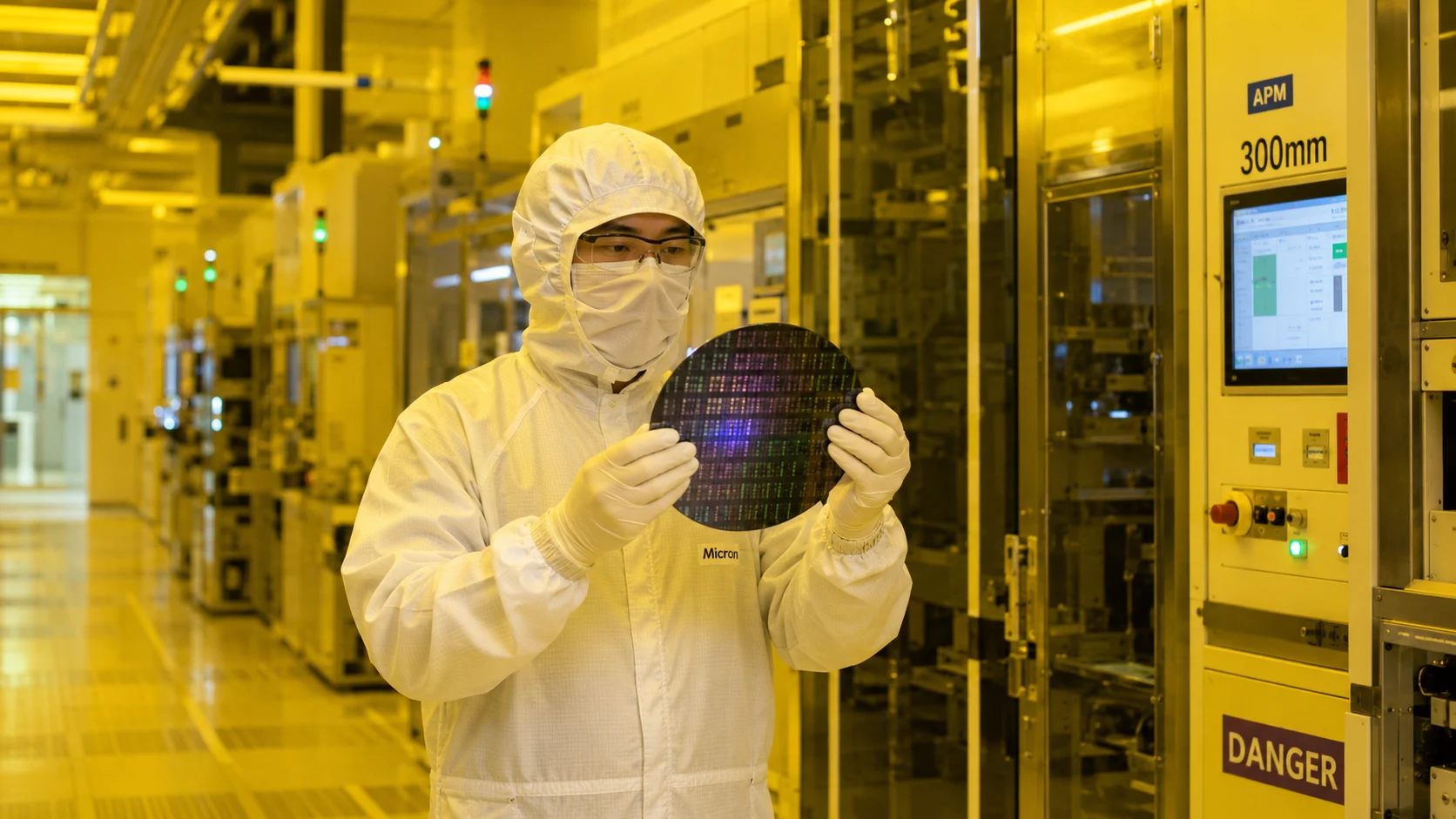
Cleanroom work and required skills
Working inside a semiconductor fab cleanroom is unlike any other manufacturing environment. The cleanroom is classified by ISO standard - most advanced logic and memory fabs operate at ISO Class 3 or ISO Class 4, meaning fewer than 1,000 or 10,000 particles per cubic meter of air respectively. To maintain that cleanliness, all workers must follow strict gowning protocols, wearing full bunny suits, gloves, hoods, booties, and face masks. Anything that sheds particles - including cosmetics, certain fabrics, and ordinary skin contact with surfaces - is prohibited. First-time fab workers almost universally describe gowning and cleanroom culture as the steepest initial adjustment.
The core wafer fabrication processes that technicians and engineers work with fall into a handful of major categories. Photolithography uses light and chemical photoresists to pattern circuit features onto the silicon wafer. Etch processes (both dry plasma etch and wet chemical etch) remove material from exposed areas. Deposition processes (chemical vapor deposition, physical vapor deposition, atomic layer deposition) add thin film layers. Chemical mechanical planarization (CMP) polishes wafer surfaces flat between layers. Metrology and inspection tools measure all of this at nanometer scales to catch defects early. An experienced technician or engineer typically specializes in one or two of these unit process areas.
Specific equipment brands matter in hiring. Fab employers often list preferred experience with tools from Applied Materials (AMAT), Lam Research, Tokyo Electron (TEL), ASML, KLA, and Hitachi. ASML's extreme ultraviolet (EUV) lithography tools are especially critical at leading-edge nodes, and engineers with EUV experience are among the most aggressively recruited globally. Technicians who have maintained or operated these specific platforms at fabs in Taiwan, South Korea, Japan, or the Netherlands are highly sought by US fabs building identical tool sets.
- Cleanroom gowning and contamination control protocols (ISO Class 3 to ISO Class 5)
- Photolithography: coat, expose, develop, etch cycles and photoresist chemistry
- Plasma etch: reactive ion etch (RIE), inductively coupled plasma (ICP), endpoint detection
- Thin film deposition: CVD, PVD, ALD process control and tool maintenance
- CMP: polish rate control, slurry chemistry, endpoint detection, post-CMP cleaning
- Metrology: CD-SEM, ellipsometry, XRF, defect inspection (KLA tools)
- Semiconductor-specific certifications: SEMI standards training, fab-internal qualification programs
- Associate or technical degree from a semiconductor manufacturing program (Maricopa Community Colleges, Austin Community College, SUNY Polytechnic)
Salary by role
Compensation at US semiconductor fabs is competitive with any manufacturing sector in the country, and the shortage of qualified workers has pushed wages higher at each new fab announcement. The figures below reflect 2025 to 2026 market data for direct fab employees at TSMC, Intel, Samsung, and Micron. Contractor employees working through staffing agencies typically earn 10 to 20 percent less than direct hires in equivalent roles. Location adjustments matter too - Phoenix and Boise have lower cost of living than the New York metro area, where Micron's Syracuse fab sits.
| Role | Level | Typical Annual Salary (USD) | Common Employer |
|---|---|---|---|
| Process Technician | Entry (0-2 yrs) | $58,000 to $72,000 | TSMC, Micron, Samsung |
| Process Technician | Senior (3-7 yrs) | $75,000 to $92,000 | Intel, TSMC, GlobalFoundries |
| Equipment Technician | Entry to mid | $60,000 to $88,000 | All major fabs |
| Yield / Metrology Technician | Mid-level | $70,000 to $95,000 | TSMC, Samsung, Micron |
| Process Engineer | Entry (BS degree) | $100,000 to $125,000 | Intel, TSMC, Samsung |
| Process Engineer | Senior (MS/PhD or 5+ yrs) | $130,000 to $160,000 | TSMC, Intel, Micron |
| Equipment Engineer | Mid to senior | $115,000 to $155,000 | All major fabs |
| Integration Engineer | Senior | $140,000 to $180,000+ | TSMC, Intel |
| Module Owner / Staff Engineer | Staff level | $160,000 to $200,000+ | TSMC, Intel |
In addition to base salary, direct employees at major fabs typically receive signing bonuses (often $10,000 to $30,000 for engineers), relocation packages, annual performance bonuses of 5 to 15 percent of base pay, and equity or profit-sharing programs. Intel and Micron are publicly traded companies with formal equity grant programs. TSMC's US subsidiary offers competitive bonuses tied to parent company performance. Total compensation packages for senior process engineers at leading-edge fabs regularly exceed $220,000 per year when all components are included.
How to apply - step by step
The path from intent to a US work authorization for a semiconductor job has several distinct stages. The steps below follow the most common sequence for a skilled technician using EB-3 or an engineer using H-1B. The exact timeline varies significantly by birth country, employer processing speed, and annual visa number availability, but the sequence itself is consistent.
- Identify target employers and roles. Use LinkedIn, the career portals of TSMC, Intel, Samsung, Micron, and GlobalFoundries, and semiconductor-specific job boards. Filter by roles that match your unit process specialization (etch, deposition, litho, CMP, metrology). Note whether job descriptions explicitly mention visa sponsorship - most major fabs do.
- Credential your experience. Gather documentation of your prior fab employment: employer letters confirming job title, dates, and responsibilities; training certificates for specific tool platforms (AMAT, Lam, TEL, ASML, KLA); any formal certifications from semiconductor training programs or SEMI standards courses. US consular officers and USCIS look for specific, verifiable evidence of the claimed two-plus years of experience.
- Engage a qualified immigration attorney. Semiconductor sponsorship involves PERM labor certification (for EB-3) or H-1B cap registration, both of which have strict procedural requirements. Major fab employers work with large immigration law firms - TSMC uses Fragomen, Intel uses multiple firms. Confirm that the employer's legal team, not a general-purpose visa agent, is handling your case.
- Complete the PERM labor certification (EB-3 route). Your employer files a PERM application with the Department of Labor documenting that they advertised the role, reviewed US applicants, and found none qualified. Current PERM processing at DOL is typically six to twelve months for a regular (non-audit) application. Certain specialty fab roles with very specific experience requirements are less likely to be audited.
- File the I-140 immigrant petition (EB-3 or EB-2). Once PERM is certified, the employer (or you, for NIW self-petition) files the I-140 with USCIS. Premium processing ($2,805 as of 2026) reduces the decision time to fifteen business days. Approval of the I-140 locks in your priority date, which is the date your place in the visa number queue is established.
- Register for H-1B lottery (H-1B route for engineers). If targeting a nonimmigrant path, your employer registers you in the annual H-1B lottery each March. Engineers at named fab sites with high wage offers have better selection odds under the wage-weighted algorithm. If selected, the employer files a full H-1B petition for a start date of October 1.
- Wait for visa number availability (EB-3 / EB-2 immigrant route). Monitor the monthly State Department Visa Bulletin for your preference category and birth country. If your country of birth is not India or China, EB-3 Skilled Worker dates are typically current or close to current. If you are born in India or China, consult an attorney about using the EB-3 Other Workers or NIW tracks or consider bridging on H-1B.
- Attend a consular interview or file adjustment of status. Once a visa number is available and your I-140 is approved, you either attend an immigrant visa interview at a US consulate in your home country or file an I-485 adjustment of status if you are already in the United States on a valid nonimmigrant visa. Successful completion results in a permanent resident card (green card) authorizing you to live and work in the United States indefinitely.
Throughout this process, stay engaged with your employer's HR and immigration teams. Large fab employers run cohort-based immigration programs with regular update cadences. TSMC Arizona, for example, has processed hundreds of transferees from its Taiwan operations and has well-developed internal procedures for managing each stage. Ask your recruiter at the start of the hiring process who the internal immigration point of contact is, and make sure you understand the expected timeline before you give notice to your current employer overseas.
व्यक्तिगत वीज़ा मार्गदर्शन प्राप्त करें
हर वीज़ा स्थिति अलग होती है। हमें अपनी स्थिति बताएं और हमारे प्रमाणित सलाहकार 24 घंटे के भीतर आपके मामले की समीक्षा करेंगे।
अक्सर पूछे जाने वाले प्रश्न
Can a fab technician without a degree get a US work visa?
Yes. The EB-3 Skilled Worker category is specifically designed for workers with two or more years of training or experience who do not hold a four-year university degree. A fab technician with documented cleanroom experience qualifies as long as a US employer sponsors the PERM labor certification and subsequent I-140 petition. H-1B is not the right path for technician roles that do not require a degree.
How long does EB-3 sponsorship take for a semiconductor technician?
The full timeline from PERM filing to green card issuance is typically 18 to 36 months for applicants born in countries other than India or China, where EB-3 visa numbers are generally current or near-current. For India-born and China-born applicants, the wait for a visa number can extend to five years or more due to per-country annual caps. The PERM certification phase itself currently takes six to twelve months at the Department of Labor.
Does TSMC Arizona sponsor visas for foreign workers?
Yes. TSMC Arizona has an active visa sponsorship program and has transferred hundreds of technicians and engineers from its operations in Taiwan on both nonimmigrant (H-1B, L-1) and immigrant (EB-3, EB-2) pathways. TSMC works with major immigration law firms and has internal HR teams dedicated to managing these transfers. Job listings on TSMC's US career portal that mention sponsorship availability confirm the employer is actively hiring foreign nationals for that role.
What is the difference between EB-3 and H-2B for construction tradespeople at fabs?
EB-3 is a permanent immigrant visa that leads to a green card. H-2B is a temporary nonimmigrant visa for non-agricultural seasonal or peak-load work, capped at 66,000 visas per year and requiring the employer to demonstrate temporary need. For fab construction projects with defined end dates, H-2B may be appropriate. For ongoing fab operations roles that will exist permanently, EB-3 is the correct pathway. Most fab employers hiring tradespeople for operations (not construction) use EB-3.
Can I apply for EB-2 NIW as a semiconductor engineer without a job offer?
Yes. The EB-2 National Interest Waiver allows self-petition without a US job offer or PERM labor certification, provided you can demonstrate that your work is of substantial intrinsic merit, has national scope, and that waiving the normal job offer requirement serves the national interest. Given the CHIPS Act's explicit national security rationale for rebuilding US semiconductor capacity, USCIS has been relatively receptive to NIW petitions from engineers with strong records in process development, EUV lithography, advanced packaging, or other areas directly tied to domestic fab capability.
Which semiconductor fab sites are hiring the most workers right now?
As of mid-2026, TSMC Fab 21 in Phoenix Arizona, Intel's Ohio One campus near Columbus, and Samsung's Taylor Texas fab are the three largest active hiring sites. Micron's Syracuse New York mega-fab is in early construction ramp and will accelerate hiring through 2027 and 2028. GlobalFoundries in Malta New York maintains steady hiring for its specialty node operations. All five sites post roles on their corporate career portals and work with US-based and international recruiting firms.
Do I need prior semiconductor experience or can I train in the US?
For EB-3 Skilled Worker sponsorship, you must demonstrate at least two years of training or work experience before the petition is filed, which means prior international experience is generally necessary. However, several US community colleges - including Maricopa Community Colleges in Arizona, Austin Community College in Texas, and SUNY Polytechnic in New York - now offer semiconductor technician certificate and associate degree programs that can qualify students for entry-level fab roles. Graduates of these programs may be eligible for EB-3 through the unskilled or other worker subcategory, though that category has longer wait times.
What tools and equipment experience gives me the best chance at a US fab job?
Experience with ASML EUV and DUV lithography systems is the single highest-demand technical credential in leading-edge fab hiring. Beyond that, hands-on operation or maintenance of Applied Materials etch or deposition tools, Lam Research Kiyo or Flex etch tools, Tokyo Electron coater-developers, and KLA inspection and metrology platforms are all highly sought. Engineers with specific module ownership experience (metal, gate, contact) at sub-7nm nodes are aggressively recruited. Certifications through SEMI, tool vendor training programs, or fab-internal qualification documentation all strengthen a visa petition by providing documentary evidence of specific technical skills.
संबंधित लेख
हमारे मुफ्त टूल्स का उपयोग करें
कनाडा CRS, ऑस्ट्रेलिया पॉइंट्स, यूके Skilled Worker, जर्मनी Opportunity Card और 34 देशों की वेतन सीमा के लिए मुफ्त कैलकुलेटर।
सभी टूल्स देखें